Java Boost Schematic Please Review My Homemade Boost Convert
Boost converter schematic diagram Keeley schematic Breadboarding a simple mosfet booster
Guitar FX Layouts: Keeley Java Boost
Schematic_5v boost resources Schematic circuit of boost converter. Question about boost schematic...
Boost boost schematic diagram
Clean boost schematic15. schematic diagram of boost converter. Please review my homemade boost converterMc34063a pinout, example circuits, datasheet, applications,, 40% off.
Boost switchGuitar fx layouts: keeley java boost Schematic diagram of the boost converter implementation.A simple dc-dc boost converter circuit using 555 timer ic.

Voltage booster circuit diagram
Schema boosteru k el. kytaře (stránka 1)4: a schematic circuit of a boost converter Schematic diagram of the boost converter implementation.Schematic diagram of the boost converter.
Simulation schematic. (a): conventional bidirectional boost-buckMosfet audio amplifier circuit diagram Keeley katana boost schematicSchematic boost converter sheet 1 20191024172646.

Boost converter circuit diagram pdf
Katana keeley boost layout rev tagboardeffects guitar delayBoost converter schematic diagram Schematic 500k pullMosfet booster amz breadboarding barbarach.
Circuit diagram of boost converterDc to dc boost converter circuit homemade Lm2577 boost converter circuit step up datasheet pinout, 59% offBoost controller adjustable blue.

Guitar fx layouts: keeley katana boost layout rev 2
Boost voltage inductor constant variable capacitorBoost schematic model. source: de almeida et al. (2022) [25 The general schematic of a boost circuitStudy on power electronics, duty cycle of a power electronics system.
Boost keeley java guitar pedal overdrive tagboardeffects layouts fxCircuit diagram of boost converter from fig. 3, during the switch is .


Simulation schematic. (a): Conventional bidirectional boost-buck
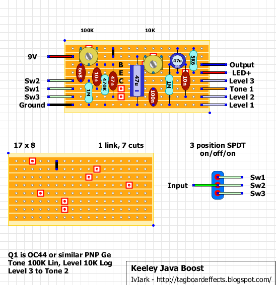
Guitar FX Layouts: Keeley Java Boost

Keeley Schematic

Schematic diagram of the Boost converter implementation. | Download

Schematic Boost Converter Sheet 1 20191024172646 | PDF | Computer

Circuit diagram of boost converter From Fig. 3, during the switch is

Clean Boost Schematic | ubicaciondepersonas.cdmx.gob.mx

Schematic_5V Boost Resources - EasyEDA